ESP8266 GPIO output performance
While building an extreme feedback device utilizing the ESP8266 and a bunch of WS2812B LEDs I missed some detailed information about the GPIO output performance of the ESP8266. This was a more general demand – but I ended up with my own WS2812 driver. And it was fun to use NOPs to achieve a nearly perfect timing (… cause I still remember the good old days when we used NOPs to create awesome rasterbars on the C64).
setup / basics
The XTENSA lx106 runs at 80 Mhz and has interrupts and watchdog disabled during measurement (see below).
Excerp from https://github.com/esp8266/esp8266-wiki/wiki/gpio-registers – I/O addresses used to control the GPIO hardware:
0x60000304 - set GPIO pin HIGH
0x60000308 - set GPIO pin LOW
0x60000310 - set GPIO pin direction output
0x60000314 - set GPIO pin direction input
Xtensa calling convention
*** this part is just here for completeness ***
The lx106 used in the ESP8266 implements the CALL0 ABI offering a 16-entry register file (see Diamond Standard 106Micro Controller brochure). By this we can apply the calling convention outlined in the Xtensa ISA reference manual, chapter 8.1.2 CALL0 Register Usage and Stack Layout:
a0 - return address
a1 - stack pointer
a2..a7 - arguments (foo(int16 a,long long b) -> a2 = a, a4/5 = b), if sizefof(args) > 6 words -> use stack
a8 - static chain (for nested functions: contains the ptr to the stack frame of the caller)
a12..a15 - callee saved (registers containing values that must be preserved for the caller)
a15 - optional stack frame ptr
Return values are placed in AR2..AR5. If the offered space (four words) does not meet the required amount of memory to return the result, the stack is used.
disabling interrupts
According to the Xtensa ISA (Instruction Set Architecture) manual the Xtensa processor cores supporting up to 15 interrupt levels – but the used lx106 core only supports two of them (level 1 and 2). The current interrupt level is stored in CINTLEVEL (4 bit, part of the PS register, see page 88). Only interrupts at levels above CINTLEVEL are enabled.
In esp_iot_sdk_v1.0.0/include/osapi.h the macros os_intr_lock() and os_intr_unlock() are defined to use the ets_intr_lock() and ets_intr_unlock() functions offered by the ROM. The disassembly reveals nothing special:
disassembly – ets_intr_lock() and ets_intr_unlock():
ets_intr_lock():
40000f74:  006320      rsil  a2, 3           // a2 = old level, set CINTLEVEL to 3 -> disable all interrupt levels supported by the lx106
40000f77:  fffe31      l32r  a3, 0x40000f70  // a3 = *mem(0x40000f70) = 0x3fffcc0
40000f7a:  0329        s32i.n  a2, a3, 0       // mem(a3) = a2 -> mem(0x3fffdcc0) = old level -> saved for what?
40000f7c:  f00d        ret.n

ets_intr_unlock():
40000f80:  006020      rsil  a2, 0           //enable all interrupt levels
40000f83:  f00d        ret.n
To avoid the overhead of the function call and the unneeded store operation the following macros to enable / disable interrupts can be used:
macros for disabling/enabling interrupts:
#define XT_CLI __asm__("rsil a2, 3");
#define XT_STI __asm__("rsil a2, 0");
NOTE: the ability to run rsil from user code without triggering a PriviledgedInstruction exception implies that all code is run on ring0. This matches the information given here https://github.com/esp8266/esp8266-wiki/wiki/Boot-Process
the watchdog
Just keep it disabled. I run into a lot of trouble with it – seemed the wdt_feed() didn’t work for me.
…and its not (well) documented at all.
Some pieces of information I found in the net:
- reverse-C of wdt_feet/task/init: http://esp8266.ru/forum/threads/interesnoe-obsuzhdenie-licenzirovanija-espressif-sdk.52/page-2#post-3505
- about the RTC memory: http://bbs.espressif.com/viewtopic.php?f=7&t=68&p=303&hilit=LIGHT_SLEEP_T#p291
gpio_output_set(uint32 set_mask, uint32 clear_mask, uint32 enable_mask, uint32 disable_mask)
declared in: esp_iot_sdk_v1.0.0/include/gpio.h
defined in: ROM (eagle.rom.addr.v6.ld -> PROVIDE ( gpio_output_set = 0x40004cd0 ))
C example:
gpio_output_set(BIT2, 0, BIT2, 0);  // HIGH
gpio_output_set(0, BIT2, BIT2, 0);  // LOW
gpio_output_set(BIT2, 0, BIT2, 0);  // HIGH
gpio_output_set(0, BIT2, BIT2, 0);  // LOW
disassembly – call to gpio_output_set(BIT2, 0, BIT2, 0):
40243247:       420c            movi.n  a2, 4                                     // a2 = 4
40243249:       030c            movi.n  a3, 0                                     // a3 = 0
4024324b:       024d            mov.n   a4, a2                                    // a4 = 4
4024324d:       205330          or      a5, a3, a3                                // a5 = 0
40243250:       f79001          l32r    a0, 40241090 <system_relative_time+0x18>  // a0 = *mem(40241090) = 0x40004cd0
40243253:       0000c0          callx0  a0                                        // call 0x40004cd0 - gpio_output_set
disassembly – gpio_output_set (thanks to By0ff for the ROM dump):
> xtensa-lx106-elf-objdump -m xtensa -EL  -b binary --adjust-vma=0x40000000 --start-address=0x40004cd0 --stop-address=0x40004ced -D 0x4000000-0x4011000/0x4000000-0x4011000.bin

0x4000000-0x4011000/0x4000000-0x4011000.bin:     file format binary

Disassembly of the .data section:

40004cd0 <.data+0x4cd0>:
40004cd0:       f0bd61          l32r    a6, 0x40000fc4  // a6 = *mem(0x40000fc4) = 0x60000200
40004cd3:       0020c0          memw                    // finish all mem operations before next op
40004cd6:       416622          s32i    a2, a6, 0x104   // mem(a6 + 0x104) = a2 -> mem(0x60000304) = 4 (SET)
40004cd9:       0020c0          memw
40004cdc:       426632          s32i    a3, a6, 0x108   // mem(a6 + 0x108) = a3 -> mem(0x60000308) = 0 (CLR)
40004cdf:       0020c0          memw
40004ce2:       446642          s32i    a4, a6, 0x110   // mem(a6 + 0x110) = a4 -> mem(0x60000310) = 4 (DIR -> OUTPUT)
40004ce5:       0020c0          memw
40004ce8:       456652          s32i    a5, a6, 0x114   // mem(a6 + 0x114) = a5 -> mem(0x60000314) = 0 (DIR -> INPUT)
40004ceb:       f00d            ret.n                   // return to the caller

> od -A x -j 0xfc4 -N 4 -x 0x4000000-0x4011000/0x4000000-0x4011000.bin
000fc4 0200 6000            // *mem(0x40000fc4) = 0x60000200
000fc8
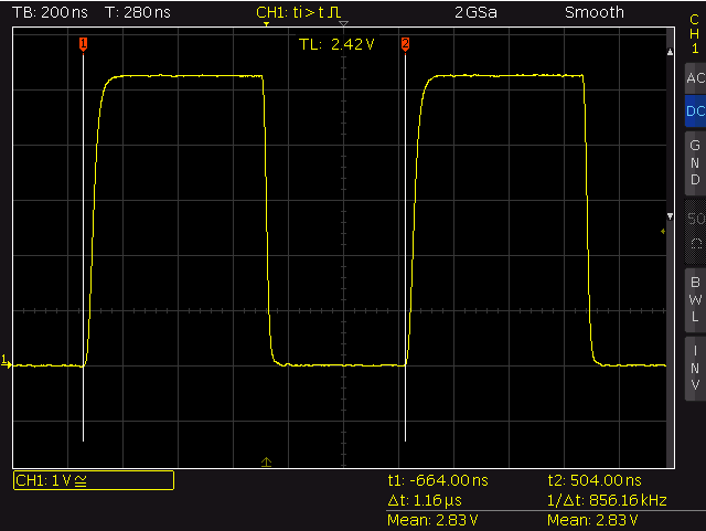
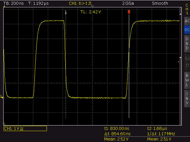
gpio_output_set()
The whole cycle of a HIGH-RISE/LOW/HIGH-RISE transition takes 1160 nano seconds – the execution of one call to gpio_output_set() takes ~580ns (~46 cycles@80Mhz). Since the clear operation is executed after the set operation (see the code above) the LOW period is slightly shorter then the HIGH period (HIGH: 675ns, LOW: 485ns). By setting an initial LOW GPIO to HIGH and LOW in the same command a short pulse of 88 nano seconds length (~7 cycles) is created.
The macro GPIO_OUTPUT_SET(gpio_no, bit_value) – defined in esp_iot_sdk_v1.0.0/include/gpio.h – is just a wrapper for gpio_output_set():
#define GPIO_OUTPUT_SET(gpio_no, bit_value) \
    gpio_output_set(bit_value<<gpio_no, ((~bit_value)&0x01)<<gpio_no, 1<<gpio_no,0)
WRITE_PERI_REG(addr, val)
Macro defined in esp_iot_sdk_v1.0.0/include/eagle_soc.h:
#define WRITE_PERI_REG(addr, val) (*((volatile uint32_t *)ETS_UNCACHED_ADDR(addr))) = (uint32_t)(val)
It boils down to the following assembly instructions:
4024323a:       080000          excw
4024323d:       600003          excw                // --> *mem(4024323c) -> 0x60000308

40243240:       000304          excw
40243243:       f03d60          subx8   a3, a13, a6 // --> *mem(40243240) -> 0x60000304

// set
40243252:       fffb21          l32r    a2, 40243240 <eagle_lwip_getif+0x28>    // a2 = 0x60000304
40243255:       230c            movi.n  a3, 4                                   // a3 = 4
40243257:       0020c0          memw
4024325a:       0239            s32i.n  a3, a2, 0                               // mem(a2 + 0) = a3 -> mem(0x60000308) = 4

// clear
4024325c:       fff821          l32r    a2, 4024323c <eagle_lwip_getif+0x24>    // a2 = 0x60000308
4024325f:       430c            movi.n  a3, 4                                   // a3 = 4
40243261:       0020c0          memw
40243264:       0239            s32i.n  a3, a2, 0                               // mem(a2 + 0) = a3 -> mem(0x60000308) = 4
To avoid optimization by the compiler I used the following hand crafted code for the measurement:
...
__asm__("movi    a2, 0x60000304  \n" // will be converted to literal load - l32r    a2, 40243240 <eagle_lwip_getif+0x28>
    "movi.n  a3, 4       \n"
    "memw           \n"
    "s32i.n  a3, a2, 0     \n"
    );

__asm__("movi    a2, 0x60000308  \n"
    "movi.n  a3, 4       \n"
    "memw           \n"
    "s32i.n  a3, a2, 0     \n"
    );
...
The disassembly shows that the movi is converted to a literal load (as expected):
...
40243248:       fffd21          l32r    a2, 4024323c <eagle_lwip_getif+0x24>
4024324b:       430c            movi.n  a3, 4
4024324d:       0020c0          memw
40243250:       0239            s32i.n  a3, a2, 0
40243252:       fffb21          l32r    a2, 40243240 <eagle_lwip_getif+0x28>
40243255:       430c            movi.n  a3, 4
40243257:       0020c0          memw
4024325a:       0239            s32i.n  a3, a2, 0
...
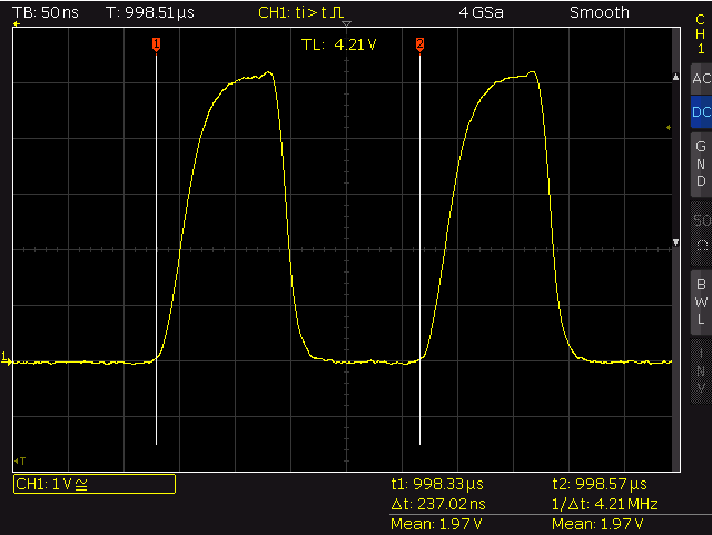
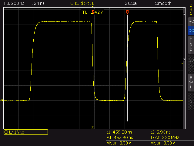
write_peri_reg()
The whole cyle of a HIGH-RISE/LOW/HIGH-RISE transition takes 237ns nano seconds with a HIGH-period
of 100 ns (8 cycles) and a LOW-period of 137 ns (11 cycles – the HIGH-period is three cycles shorter
then the LOW period – maybe caused by one additional instruction fetch).
By avoiding the mov and removing the memw operations I was able to generate pulses with a period time of 150ns (12 cycles, HIGH: ~52ns, LOW: ~98ns).
__asm__("movi    a2, 0x60000304  \n"
    "movi    a4, 0x60000308  \n"
    "movi.n  a3, 4       \n"  // GPIO2
    "memw           \n"
    "s32i.n  a3, a2, 0     \n"
    "s32i.n  a3, a4, 0     \n"
    "s32i.n  a3, a2, 0     \n"
    "s32i.n  a3, a4, 0     \n"
    "s32i.n  a3, a2, 0     \n"
    "s32i.n  a3, a4, 0     \n"
  );
fastest – T: ~150ns
WS2812B timing
…this was the starting point that forced me to have a deeper look into that topic. There are already some implementations for controlling the WS2812B. They work – just use them. This part is for fun and education … ahh, lets do it in plain assembly.
static inline void WS2812B_SEND_1(int port)
{
  //800ns HIGH & 450ns LOW
  __asm__ volatile ("movi    a2, 0x60000304  \n"
            "movi    a3, 0x60000308  \n"
            "movi    a4, %0      \n"
            "s32i    a4, a2, 0     \n"
            "memw            \n"
            "movi    a5, 14         \n"
            "3:            \n"
            "addi    a5, a5, -1    \n"
            "bnez    a5, 3b      \n"
            "nop.n           \n"
            "nop.n           \n"
            "nop.n           \n"
            "nop.n           \n"
            "nop.n           \n"
            "s32i    a4, a3, 0     \n"
            "memw            \n"
            "movi    a5, 2         \n"
            "4:            \n"
            "addi    a5, a5, -1    \n"
            "bnez    a5, 4b      \n"
           :: "g" (port)
           : "a2", "a3", "a4", "a5"
           );
}
ws2812b – send logical 1
SEND_1_HIGH: 796ns
SEND_1_LOW:  454ns
static inline void WS2812B_SEND_0(int port)
{
  //400ns HIGH & 850ns LOW
  __asm__ volatile ("movi    a2, 0x60000304  \n"
            "movi    a3, 0x60000308  \n"
            "movi    a4, %0      \n"
            "s32i    a4, a2, 0     \n"
            "memw            \n"
            "movi    a5, 7         \n"
            "1:            \n"
            "addi    a5, a5, -1    \n"
            "bnez    a5, 1b      \n"
            "nop.n           \n"
            "s32i    a4, a3, 0     \n"
            "memw            \n"
            "movi    a5, 10         \n"
            "2:            \n"
            "addi    a5, a5, -1    \n"
            "bnez    a5, 2b      \n"
            "nop.n           \n"
            "nop.n           \n"
              "nop.n           \n"
           :: "g" (port)
           : "a2", "a3", "a4", "a5"
           );
}
ws2812b – send logical 0
SEND_0_HIGH: 397ns
SEND_0_LOW: 855ns
experiences
- Add a ~400 ohm resistor into the WS2812 data input line to avoid oscillation caused by reflections of the input of the first LED.
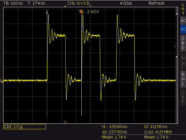
write_peri_reg() – no resistor
- Use decoupling capacitors – without I got strange noise on the power supply line.
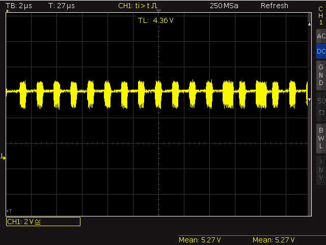
pwr supply – noise bursts
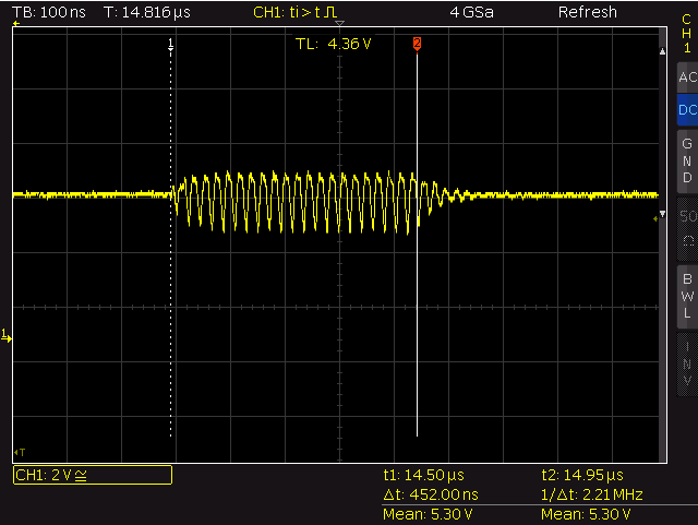
pwr supply – single bursts
- Ensure the WS2812 data line uses a proper signal level. According to the data sheet DATA_IN is treated as HIGH above 3.5V (0.7*Vdd) and LOW below 1.5V (0.3*Vdd)). The Vhigh of 3.3V offered by the ESP9266 is not enough for the WS2812B to be detected as a clean HIGH signal (I got some strange flickers – after adding a 4050 as level shifter everything was fine).
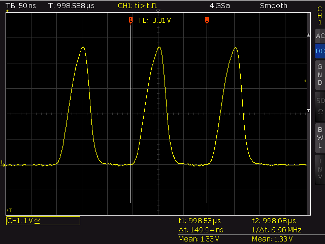
- Disable interrupts during bit-banging the WS2812. Avoid disabled interrupts for more then 10ms or wireless connections will act wired. Keeping that in mind you will be able to write ~300 LEDs at once (1250ns per bit, 8 bit per color, 3 colors = 30us, internal overhead when switching to the next pixel = 225ns, keep 50us between each write for reset condition). If you need to run the code from above from flash check the timing using an oscilloscope. I have seen NOPs taking more then one cycle…
- Wear sunscreen.